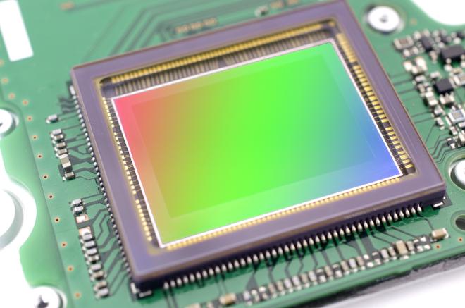
Photography CMOS image Sensor

Table of Contents
CMOS Imaging Sensor for Photography #
Overview #
This project focused on the development of a high-frame-rate CMOS imaging sensor capable of up to 8K resolution, targeting the professional photography market. The work involved designing the sensor’s architecture and implementing its high-speed interfaces: SLVS-EC and MIPI. Contributions spanned the entire design cycle, from architecture definition and RTL implementation to verification and backend integration.
Key Features and Achievements #
- Sensor Architecture:
- Collaborated on crafting the overall architecture for the 8K CMOS sensor, optimizing for high resolution and frame rate.
- Interface Design:
- Designed and implemented the SLVS-EC and MIPI interfaces for high-speed data transfer.
- Design Implementation:
- Developed and verified RTL using VHDL for all digital components.
- Assisted in defining and applying detailed timing constraints to achieve successful timing closure.
- Supported backend synthesis to ensure the design met performance and area requirements.
- Verification:
- Contributed to the verification process, ensuring robust and error-free operation.
- Wrote various UVM testbenches and reusable blocks
- Toolchain Utilization:
- Used the Cadence toolchain (Genus, Xcelium, Innovus, and Tempus) for synthesis, simulation, backend, and timing analysis.
Technical Details #
- High-Performance Interfaces:
- Implemented SLVS-EC for efficient, low-power, and scalable data transmission.
- Integrated MIPI for compatibility with mobile and photography industry standards.
- RTL Development:
- Focused on modular and efficient design for the sensor’s digital blocks, targeting low latency and high throughput.
- Backend and Timing:
- Ensured synthesis and timing closure through rigorous iterations using Cadence tools.
- Developed timing constraints to guide placement and routing for optimal performance.
- Verification Efforts:
- Supported the development of a comprehensive testbench to validate the sensor’s functionality and performance.
Challenges and Solutions #
- High-Speed Data Transmission: Overcame challenges in designing high-speed interfaces by optimizing the implementation of SLVS-EC and MIPI standards.
- Timing Closure: Addressed timing challenges through careful constraint definition and iterative backend runs.
- System Integration: Balanced architectural design with implementation needs to ensure smooth integration of all components while meeting strict performance targets.
Outcome #
The project successfully delivered a high-frame-rate, 8K CMOS imaging sensor tailored for the professional photography market. With robust high-speed interfaces and efficient architecture, the sensor achieved exceptional performance, meeting stringent industry standards. Contributions across the design cycle, from RTL to backend, ensured a reliable and high-quality outcome.